In a significant advancement that could reshape the global semiconductor landscape, China has successfully developed a prototype of an extreme ultraviolet (EUV) lithography machine through entirely domestic efforts. Achieved in early 2025, this milestone marks a critical step in Beijing’s quest for technological self-sufficiency amid escalating US-led export restrictions. The prototype, constructed in a high-security facility in Shenzhen, demonstrates China's growing capability to replicate technology previously monopolized by the Dutch giant ASML.
The Path to the Prototype: Reverse Engineering and Strategic Talent
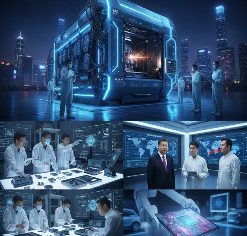
The development of China’s EUV machine has been likened to a modern-day "Manhattan Project," involving thousands of engineers and a coordinated network of state-backed research institutes and private firms.
Talent Recruitment: A core team was formed by recruiting former ASML engineers—many of whom are Chinese-born—using lucrative incentives such as signing bonuses ranging from 3 to 5 million yuan (approximately $420,000 to $700,000) and housing subsidies.
Operational Secrecy: The project operated under extreme confidentiality. Employees reportedly used aliases and fake IDs to maintain security.
Sourcing Components: The team reverse-engineered technology by disassembling older machinery. Parts were sourced through secondary markets, auctions, and even restricted components from Japanese firms.
Physical Scale: The prototype is massive, occupying nearly an entire factory floor—significantly larger than ASML’s standard systems, which weigh roughly 180 tons.
While the machine successfully generates the necessary EUV light—a plasma created by blasting molten tin with lasers—it has yet to produce functional, market-ready chips.
Key Institutional Players
Several organizations have been instrumental in reaching this stage:
Changchun Institute of Optics, Fine Mechanics and Physics (CIOMP): Focused on light sources and optical systems.
Shanghai Institute of Optics: Contributed pivotal research and patent filings.
Huawei: Acted as a primary coordinator for the supply chain, despite being on the US entity list. CEO Ren Zhengfei reportedly provides direct progress updates to senior national leadership.
Technical Hurdles and Ongoing Challenges
Despite this success, replicating ASML’s decades of refinement remains a daunting task. ASML invested over $7 billion and nearly twenty years to commercialize its first EUV system.
Challenge | Impact on Production |
|---|---|
Precision Optics | China struggles to match the quality of lenses supplied by Germany’s Carl Zeiss AG. |
Mechatronics | Achieving the ultraprecise movement required for 2-nm chips is complex. |
| Yield & Throughput | Generating light is only the first step; doing so at an economically viable scale is much harder. |
Legal Issues | The project has been shadowed by allegations of trade secret theft and intellectual property disputes. |
Government Strategy and Global Impact
This initiative is a centerpiece of China’s broader semiconductor strategy, overseen by the Central Science and Technology Commission. The goal is to eliminate Western influence from the domestic supply chain.
Timeline: The government aims for working chips by 2028, though independent analysts suggest 2030 is a more realistic target for mass production.
Market Share: Currently, domestic suppliers meet only about 1.5% of China’s lithography demand, with ASML and Japanese firms controlling 99% of the market.
Geopolitical Leverage: Mastery of EUV technology would grant Beijing significant influence in both the global economy and defense sectors, particularly regarding AI and high-performance computing.
As the US-China "chip war" intensifies, the world is watching to see if this prototype can evolve into a production powerhouse. If successful, China may achieve semiconductor independence years ahead of Western predictions, challenging global monopolies and shifting the balance of technological power.
 |  |  |
 |  |  |